
Introduction
Bitcoin mining hardware has spent years chasing the same basic goal: more computing power with less electricity.
That race has pushed mining chips toward increasingly smaller manufacturing processes. As chip density improves, manufacturers can fit more computing power into a smaller area while, in many cases, reducing the energy required to perform each terahash.
But there is another part of the semiconductor industry that rarely gets much attention from miners: the machines used to manufacture those chips.
This is where Japanese technology company Canon enters the picture.
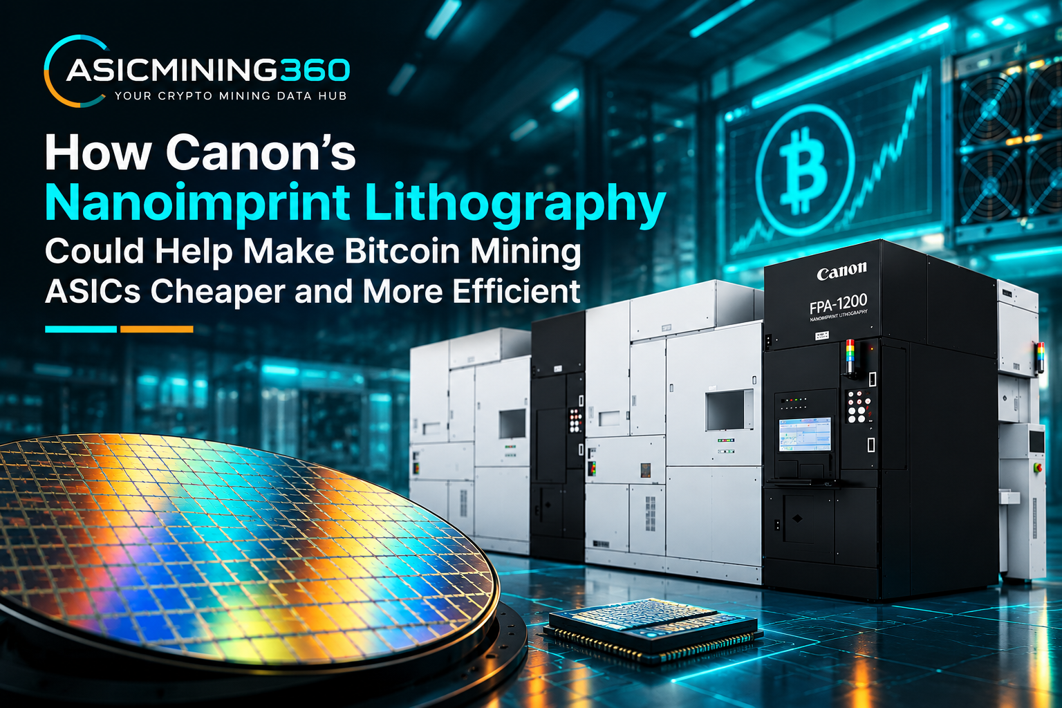
Canon is developing nanoimprint lithography (NIL) as an alternative to conventional optical lithography. Its approach is very different from the technology used in today's leading-edge semiconductor fabs. More importantly, Canon's latest developments raise an interesting question for the Bitcoin mining industry: could a different way of manufacturing advanced chips eventually help produce more affordable and efficient mining ASICs?
What Is Canon’s Nanoimprint Lithography?
Traditional photolithography works somewhat like projecting a highly precise image onto a wafer. Light passes through an optical system and transfers the circuit pattern onto a layer of resist.
Canon's NIL system takes a different approach.
Instead of projecting the pattern with light, a template carrying the circuit design is pressed directly into the resist on the wafer, much like a microscopic stamp. The pattern is physically transferred to the wafer rather than projected through a complex optical system.
Canon's FPA-1200NZ2C can produce patterns with a minimum linewidth of 14 nm. Canon says this is equivalent to the resolution associated with a 5-nm process node and that improvements in mask technology could eventually allow 10-nm linewidth patterning, corresponding to a 2-nm node.
That does not mean the machine itself is a 5-nm or 2-nm chip factory. Semiconductor process nodes involve far more than lithography resolution. Still, the figures show why Canon's technology has attracted attention in advanced semiconductor manufacturing.
Canon vs. ASML: Two Different Paths
Canon is sometimes described as a challenger to ASML, but that comparison needs some qualification.
ASML's leading systems use extreme ultraviolet lithography (EUV) to produce some of the world's most advanced logic chips. Canon's NIL system is based on a fundamentally different process. It does not try to reproduce EUV exposure with another optical method. Instead, it avoids the exposure step and physically stamps the pattern onto the wafer.
That difference could matter because advanced lithography equipment is extremely complicated and energy intensive.
Canon says its NIL process can significantly reduce power consumption because it does not require the specialized light source used by advanced optical lithography. The company has also presented NIL as a technology with the potential to reduce semiconductor manufacturing costs.
Canon has estimated that, for a 15-nm patterning process, NIL could reduce wafer manufacturing costs by around 23% compared with EUV, while the energy used for the patterning process could fall by roughly 87%.
Those figures are Canon's estimates under specific conditions, not a guarantee that every advanced chip will be 23% cheaper to manufacture. Still, they point to one of the technology's most interesting advantages.
Why Lithography Matters for Bitcoin Mining ASICs
For a Bitcoin miner, the lithography machine is several steps removed from the final product.
A mining company such as Bitmain designs an ASIC around the SHA-256 workload. The actual chip is then manufactured by a semiconductor foundry using a particular process technology.
So Canon is not making Bitcoin mining chips. It is making equipment that could potentially be used by semiconductor manufacturers that produce chips for companies such as mining hardware designers.
The reason lithography still matters to miners is simple: the manufacturing process influences how much computing performance can be packed into a chip and how efficiently that chip can operate.
Bitcoin mining is unusually sensitive to this relationship because electricity is one of the largest operating expenses for a mining farm. A chip that performs more hashing for every joule can directly affect the economics of a mining operation.
But energy efficiency is not the only economic factor.
The price of the ASIC itself matters.
Could NIL Eventually Make Bitcoin Mining ASICs Cheaper?
This is where Canon's technology becomes particularly interesting for the mining industry.
Modern Bitcoin mining machines can contain a large number of semiconductor components, and the mining chips themselves represent a significant part of the hardware's manufacturing cost. As mining machines become more powerful, the bill for advanced silicon becomes increasingly important.
Some high-end Bitcoin mining machines have already reached prices of $12,000–$13,000 or more, depending on the model, configuration, market conditions and seller. At those prices, the initial capital required to deploy a single machine can become a major part of the mining equation.
That matters because a miner does not simply need an efficient machine. The machine also needs to earn back its purchase price.
Imagine a future in which an advanced manufacturing process such as NIL can produce suitable mining chips at a lower wafer cost. The saving would not necessarily appear directly as a 23% reduction in the retail price of an Antminer or WhatsMiner. The final machine price also includes chip packaging, memory and other components, power supplies, cooling systems, assembly, logistics, research and development, manufacturer margins and market demand.
Even so, a cheaper chip could create room for a cheaper mining machine.
For example, if a future ASIC manufacturer could obtain the same class of computing performance while spending less on wafer production, part of that saving could potentially be passed on to customers. Alternatively, the manufacturer could keep the machine's price similar while delivering more computing power or a better efficiency figure.
For miners, either outcome could be valuable.
A lower purchase price means less capital is tied up in hardware. If the machine generates roughly the same daily mining revenue, a lower upfront cost can shorten the time required to recover the original investment.
That is especially relevant when mining profitability is under pressure. Bitcoin mining economics can change quickly when the Bitcoin price falls, network difficulty rises, or electricity costs increase. A machine that costs several thousand dollars less to purchase has a different risk profile from an otherwise similar machine with a much higher upfront price.
In other words, NIL could potentially affect Bitcoin mining economics from two directions: manufacturing efficiency and hardware cost.
Could It Improve ASIC Mining ROI?
The answer is potentially yes, but it needs to be framed correctly.
A cheaper ASIC does not automatically produce more Bitcoin. It does not make the machine more electrically efficient by itself, either.
However, if NIL eventually helps reduce the cost of producing the underlying mining chips, the effect could reach the miner through a lower hardware price.
Consider two otherwise similar machines. If Machine A costs $13,000 and Machine "B" costs $10,000 while providing comparable hashrate and energy efficiency, Machine B starts with a $3,000 lower capital burden.
That difference can be meaningful when calculating payback time.
Just do the math: if a machine pulls in $10 of clear profit a day after electricity, paying a $3,000 premium upfront means you need about 300 extra days of mining just to close the gap.
Obviously, your real-world mileage will vary. BTC price action, mining difficulty, and energy costs change constantly. But the baseline rule of thumb doesn’t.
This is why semiconductor manufacturing technology can matter to Bitcoin miners even when miners never see the lithography machine itself.
The benefit could eventually arrive as a lower price tag on the finished ASIC.
Could Bitmain, MicroBT and Canaan Benefit?
In theory, yes—if the foundries producing their chips adopt NIL for suitable production processes.
Bitmain and other mining hardware companies do not normally need to own the lithography equipment themselves. They depend on semiconductor manufacturing partners and their process technologies.
That means Canon's potential impact would be indirect.
If a foundry found NIL suitable for producing a particular generation of high-performance logic chips, ASIC designers could eventually have another manufacturing option. That could matter to companies such as Bitmain, MicroBT and Canaan if their manufacturing partners adopted the technology.
However, Bitcoin mining ASICs are not ordinary consumer processors.
They are highly specialized chips designed around a narrow workload. Their economics depend on the complete package—from chip design and wafer production to packaging, power delivery and cooling.
NIL would therefore have to fit into that larger manufacturing chain before miners would notice a meaningful benefit.
Canon Is Also Working Beyond Lithography
Canon's semiconductor work is becoming broader than NIL itself.
In January 2026, the company announced inkjet-based adaptive planarization (IAP), a technique designed to smooth wafer surfaces by applying material according to the wafer's existing topography and then pressing a flat glass plate onto it. Canon says the process can reduce topographical irregularities to 5 nm or less on 300-mm wafers. The company plans to commercialize equipment incorporating the technology in 2027.
This is relevant because advanced chips are built through many layers of materials and wiring. Small surface irregularities can create alignment problems as more layers are added.
Canon is therefore working on several pieces of the semiconductor manufacturing process that could become increasingly important as chips become more complex.
The Limits: Why Canon Is Not Replacing EUV Yet
It’s tempting to look at Canon’s NIL technology and hype it up as the ultimate 'ASML killer.' But let's not get ahead of ourselves.
Even Canon admits that NIL is still finding its footing for true mass production. Right now, fabs are still tweaking their setups, while Canon works out the kinks with mask durability, cleaning, and overall process integration. Meanwhile, ASML remains the undisputed king when it comes to churning out the world's most advanced logic chips.
The real question isn't whether Canon is going to dethrone ASML overnight. It’s whether chipmakers will start mixing and matching their lithography tech depending on the specific job. If NIL can prove it's both reliable and cost-effective at scale, it could absolutely carve out a solid spot in that mix.
What Canon’s Technology Could Mean for Bitcoin Mining Hardware
For Bitcoin miners, Canon's NIL technology is worth watching—not because Canon is entering the mining-machine business, but because the battle for mining efficiency starts long before an Antminer or WhatsMiner reaches a mining farm.
Every generation of mining hardware depends on improvements somewhere in the semiconductor supply chain.
If NIL can mature into a cost-effective, reliable process for advanced logic manufacturing, it could give chipmakers another tool for producing dense and efficient silicon. More importantly, it could potentially lower some of the manufacturing costs behind those chips.
That could eventually translate into less expensive mining hardware, shorter capital-recovery periods and a lower entry barrier for miners.
But none of this is guaranteed. The final price of an ASIC depends on many factors beyond the cost of the silicon itself, and there is no certainty that a saving at the wafer level would be passed entirely to the customer.
Still, the possibility is worth watching.
Bitcoin mining has become a race not only for better hash efficiency, but also for better hardware economics. The next meaningful improvement may not always come from a new cooling system or a faster ASIC architecture. It could come from a manufacturing technology sitting several steps behind the finished machine.
Canon's nanoimprint lithography is one of the technologies that could eventually influence that equation.