Every device you touch daily—smartphone, game console, laptop, or server—relies on a processor to make decisions and move data. In high-performance environments like crypto mining and AI compute, those processors become the heart of an industrial system: they consume megawatts, generate enormous heat, and decide whether an operation is profitable or not.
At first glance, a 1980s home computer chip and a modern system-on-chip used in data centers seem to have nothing in common. One counted its transistors in the thousands and ran at a few hundred thousand operations per second. The other packs tens of billions of transistors and performs trillions of operations every second. Yet, beneath this massive gap in scale, they still follow the same fundamental ideas.
Understanding that shared foundation is not just academic. It helps miners, AI operators, and infrastructure investors make better decisions about hardware selection, cooling, power delivery, and long-term efficiency.
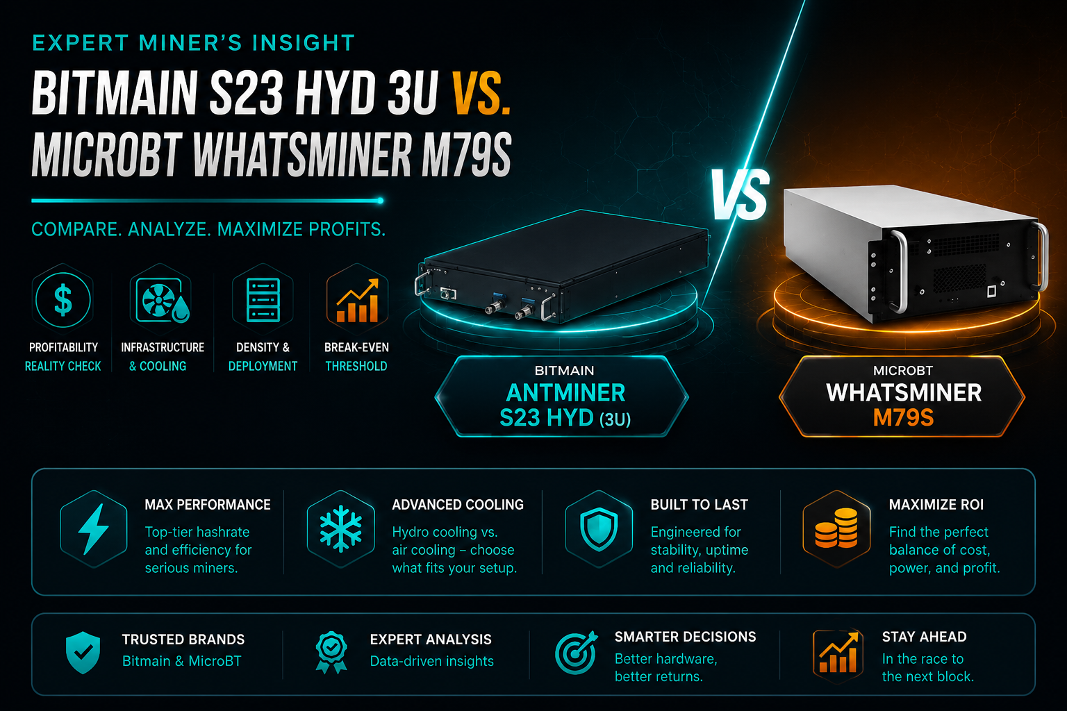
CPU vs. ASIC vs. Computer Systems: A Complete Hardware Comparison Guide
| Aspect | Computer System | CPU (General Purpose) | ASIC (Mining Specific) |
|---|---|---|---|
| Definition | Full stack: CPU, RAM, Storage, Motherboard, PSU, and OS. | The "Brain" designed to handle any software or task. | Custom hardware built for one specific algorithm (e.g., SHA-256). |
| Operation | Coordinates data across multiple hardware interfaces. | Instruction-based: Fetch-Decode-Execute cycle. | Hardwired dataflow: Logic gates are fixed for one math path. |
| Flexibility | Extreme: Runs any application imaginable. | High: Can be reprogrammed for any logic. | Zero: Cannot do anything other than its target task. |
| Performance | Highly variable depending on component synergy. | Average for hashing; overhead from decoding instructions. | Industry Lead: Highest hash rate per watt consumed. |
| Application | Workstations, Servers, Gaming, Daily computing. | Operating Systems, background tasks, complex math. | Industrial-scale Crypto Mining and Data verification. |
| Lifecycle | Easy to upgrade individual parts (Modular). | Upgradeable by swapping the chip or socket platform. | Disposable/Static: When difficulty rises, hardware becomes obsolete. |
| Risks | Software vulnerabilities and driver conflicts. | Thermal throttling and architectural bottlenecks. | Voltage instability and extreme heat density. |
The Evolution of Computing Power: From the MOS 6502 to Modern AI Clusters
To appreciate where we are today, it helps to look back briefly. Early personal computers and consoles relied on extremely simple processors by modern standards. A classic example is the MOS 6502, a chip used in many early systems like the Commodore 64, Atari consoles, and the Apple II family. It was built from just over four thousand transistors and could execute a few hundred thousand basic operations per second. Its software was limited to simple games and productivity tools, but it defined an entire generation of computing.
Fast forward several decades, and a modern laptop or server chip integrates on the order of fifteen to eighteen billion transistors. These processors can sustain multiple trillion operations per second, enabling realistic 3D graphics, real-time video processing, and large-scale machine learning workloads.
Despite this difference in raw capability, the underlying operational model is still recognizable. Whether you open a smartphone, a gaming console, a GPU card, an ASIC miner, or an AI accelerator board, you will find designs built around the same core principle: fetch instructions, interpret them, execute operations, and repeat—at extreme speed.
This is what we can call the “technological DNA” of general-purpose computing.
Inside the Chip: Understanding Modern Processor Architecture and Components
If you open a modern laptop or server board, you will not see a single “chip” in the simple sense. Instead, you find a complex package:
- A protective heat spreader to move heat away from the silicon
- An interposer or substrate with thousands of microscopic connections
- One or more silicon dies containing the real logic
- Nearby memory chips (for example DRAM) that serve as working memory
On the silicon die itself, the design is divided into many functional regions: high-performance cores, efficiency-oriented cores, cache memory blocks, memory controllers, and often integrated graphics or specialized accelerators.
If you zoom down to the nanoscopic level, you find dense layers of metal wiring and transistors. Small groups of transistors form logic gates, and those gates combine into adders, comparators, registers, and control circuits. Even in a chip with more than ten billion transistors, the basic building blocks are still the same simple components—just replicated and organized at an enormous scale.
How a CPU Works: The Workshop Analogy for Understanding Compute Logic
People often say a CPU is “just a very fast calculator.” That description misses most of the story. A more useful mental model is a workshop:
- The warehouse is your long-term storage (SSD or flash). It holds huge amounts of data, but accessing it is relatively slow.
- The cart is system memory (DRAM). It moves batches of data closer to the worker. Faster than the warehouse, but still not instant.
- The workbench is the processor core and its cache. Space is limited, but everything here is extremely fast.
- The notepad is the set of registers, where the most active values are kept.
- The tools are the execution units, especially the ALU (Arithmetic Logic Unit), which performs arithmetic and logical operations.
- The foreman is the control unit, deciding what task comes next and which tool should be used.
In this workshop, the foreman repeatedly follows a simple routine: bring in the next instruction, understand what it means, perform the operation, and record the result. This loop never stops while the system is powered on.
How Software Commands Work: The Role of Instructions and Program Counters
At the lowest level, software is not “apps” or “websites.” It is a long sequence of very small instructions. Each instruction might say something like:
- Load a value from memory into a register
- Add two registers together
- Compare two values
- Jump to another instruction if a condition is met
- Store a result back to memory
To keep track of where it is, the processor uses a special register often called the program counter (or instruction pointer). This register holds the address of the next instruction to execute. After an instruction finishes, the program counter usually moves forward—unless a jump or branch instruction tells it to go somewhere else.
This is how loops and conditional logic are built. A simple “for” loop in a high-level language becomes a sequence of loads, comparisons, conditional branches, and jumps. From the processor’s point of view, it is just following addresses and flags.
Interestingly, even modern processors do not rely on an infinite variety of instructions. Early chips like the 6502 had only a few dozen different instruction types. Today’s mainstream architectures have a few hundred. That is enough to express everything from a spreadsheet calculation to a neural network inference pipeline.
Understanding the CPU Cycle: Why Fetch, Decode, and Execute Still Matter
Almost every general-purpose processor follows the same three-step rhythm:
- Fetch – Read the next instruction from memory using the address in the program counter.
- Decode – Interpret the instruction and generate the control signals needed to perform it.
- Execute – Carry out the operation: move data, perform a calculation, compare values, or write a result.
After that, the cycle repeats with the next instruction.
In practice, modern CPUs extend this model with extra stages such as memory access and write-back, but the conceptual loop remains the same. This cycle is the reason software written decades ago can still be understood in principle: the machine model has evolved, but not been replaced.
Why CPU Clock Speed Isn’t Everything: The Truth About Gigahertz and Performance
Older processors ran at clock speeds measured in megahertz, meaning each step took about a microsecond. Modern chips operate at several gigahertz, with each cycle lasting only a fraction of a nanosecond. They also moved from 8-bit or 16-bit data paths to 64-bit architectures, allowing them to handle much larger values and memory spaces natively.
However, performance is no longer about clock speed alone. A modern core can process multiple instructions in parallel, reorder operations internally, and keep many execution units busy at once. Techniques like pipelining allow different stages of multiple instructions to overlap, increasing throughput without increasing clock frequency.
For operators in mining or AI, this is an important lesson: headline frequency numbers rarely tell the full story. Architecture, memory access patterns, and parallelism matter just as much.
Solving the Memory Wall: How ISA and Micro-Ops Impact Real-World Speed
There is another level most users never see: the distinction between the instruction set architecture (ISA) and what happens inside the core. A single “instruction” visible to software can be broken down internally into several micro-operations. These micro-ops may be executed in parallel by different units, then combined into a final result.
This approach improves performance, but it also highlights a major modern constraint: the memory wall. In many workloads—especially AI and data analytics—the bottleneck is no longer computation, but how fast data can be moved between memory, caches, and execution units.
That is why modern processors invest heavily in:
- Multi-level cache hierarchies
- High-bandwidth memory controllers
- Fast interconnects between cores and accelerators
In GPU farms and AI clusters, memory capacity and bandwidth often limit real-world performance more than raw compute power.
ASIC vs. FPGA: Why Fixed Dataflow Wins in Industrial Crypto Mining
The classic fetch–decode–execute model is extremely flexible, but flexibility costs energy and silicon area. You need instruction decoders, branch predictors, complex control logic, and large caches. All of that consumes power.
ASIC miners take a different approach. Instead of supporting many instruction types, they implement a fixed dataflow optimized for a single algorithm, such as SHA-256. Data streams through a predefined sequence of logic blocks. There is no need to fetch or decode instructions for each step—the hardware already “knows” what to do.
The result is:
- Much higher energy efficiency per unit of work
- Very high throughput for one specific task
- Almost no flexibility if the algorithm changes
FPGAs sit somewhere in between. They can be reconfigured to implement different data paths, but they are usually less efficient and more expensive per unit of performance than a purpose-built ASIC at scale.
GPUs and AI Accelerators: Parallelism at Industrial Scale
GPUs and modern AI accelerators are designed for massive parallel workloads. They excel when the same operation must be applied to huge volumes of data—exactly the case in graphics rendering, matrix math, and neural networks.
However, their real-world performance is often limited by:
- Memory bandwidth
- Memory capacity (VRAM or HBM)
- Interconnect speed between devices (PCIe, NVLink, high-speed networking)
This is why AI clusters frequently spend as much on memory and networking as on compute silicon itself. The processor may be fast, but without a steady flow of data, it sits idle.
Practical Lessons for Mining and AI Operations
Understanding these fundamentals leads to several concrete recommendations:
- Data Movement Matters as Much as Compute
In both mining management software and AI pipelines, inefficient data handling can waste expensive hardware cycles. Optimize memory layouts, reduce unnecessary transfers, and watch for bottlenecks outside the main compute loop.
- Watch the Pipeline, Not Just the Peak Numbers
A system that looks powerful on paper can underperform if it is frequently stalled by memory waits, thermal throttling, or unstable power delivery. Continuous monitoring of effective frequency, error rates, and temperatures is critical.
- Thermal Design Is a Performance Feature
Every watt becomes heat. Poor airflow or inadequate cooling leads directly to reduced clocks and lower uptime. In dense ASIC or GPU installations, disciplined airflow management or liquid/immersion cooling can make the difference between stable operation and constant throttling.
- Efficiency Is Won in the Details
Two farms with the same hardware can have very different costs due to power losses, PSU efficiency, cable sizing, cooling strategy, and operational discipline. Always measure real consumption at the wall, not just reported chip power.
Summary: Mastering Hardware Synergy for Mining and AI Success
We often judge computing power by numbers like hashrate or FLOPS, but real performance is about the bigger picture. A great chip is useless if it's held back by poor cooling, unstable power, or bad data flow.
Whether it's CPUs, ASIC miners, or AI accelerators, the secret to high performance isn't just raw power—it's synergy. If you operate in mining or AI, you can't just buy hardware based on specs alone. You need to know how it survives the heat and heavy workloads of real-world use.
Ultimately, a balanced, well-optimized system will always outperform a stronger, poorly managed one. Stop guessing and start measuring—use up-to-date tools to track your actual efficiency, power costs, and profits so you can make decisions backed by solid data.
Frequently Asked Questions (FAQ)
Q1: Does a higher transistor count always mean a faster processor?
In theory, yes, because more transistors allow the chip to do more work simultaneously. However, it’s not the whole story. Think of it like a massive engine in a car stuck in a traffic jam. If your memory (RAM) is slow or your software isn't optimized, those billions of transistors will just sit idle. Real-world speed comes from the synergy between the processor, its cooling system, and how fast data can actually reach the core.
Q2: Why don't we use ASICs in home computers if they are so fast?
Because an ASIC is "brilliant at one thing and useless at everything else." It is hardwired for a specific mathematical path. Your PC needs to switch between writing a document, browsing the web, and playing a video. This requires the versatility of a CPU. An ASIC miner might be a world champion at hashing SHA-256, but it literally cannot open a simple text file.
Q3: What exactly is the "Memory Wall" everyone talks about?
Imagine a world-class chef (the processor) who can chop vegetables in one second, but the assistant (the memory) takes a full minute to bring the vegetables from the fridge. The chef spends most of his time waiting. That is the Memory Wall. Processors have become so fast that memory technology is struggling to keep up, often making the data transfer speed the true bottleneck of your system.
Q4: Is overclocking a good idea for Mining or AI workloads?
It’s a double-edged sword. In industrial environments, stability is king. Overclocking generates massive heat, which eventually leads to thermal throttling—where the chip slows itself down to prevent melting. Usually, providing a rock-solid cooling environment and running at factory speeds yields better long-term profits than pushing the hardware to its breaking point.
Q5: How can I tell if my system has a "Data Bottleneck"?
If your CPU or GPU usage is low, but the system feels "heavy" or slow, you likely have a bottleneck in data movement. This could be due to slow storage (SSD/HDD), limited memory bandwidth, or even network latency in cloud-based AI tasks. A powerful processor can only work on the data it has actually received.