Introduction
The race to build better AI hardware is no longer just about making chips faster. It is now about designing entire computing platforms that can handle huge models, move data efficiently, and scale across large clusters without wasting power. That is exactly where AMD’s Instinct MI300 stands out.
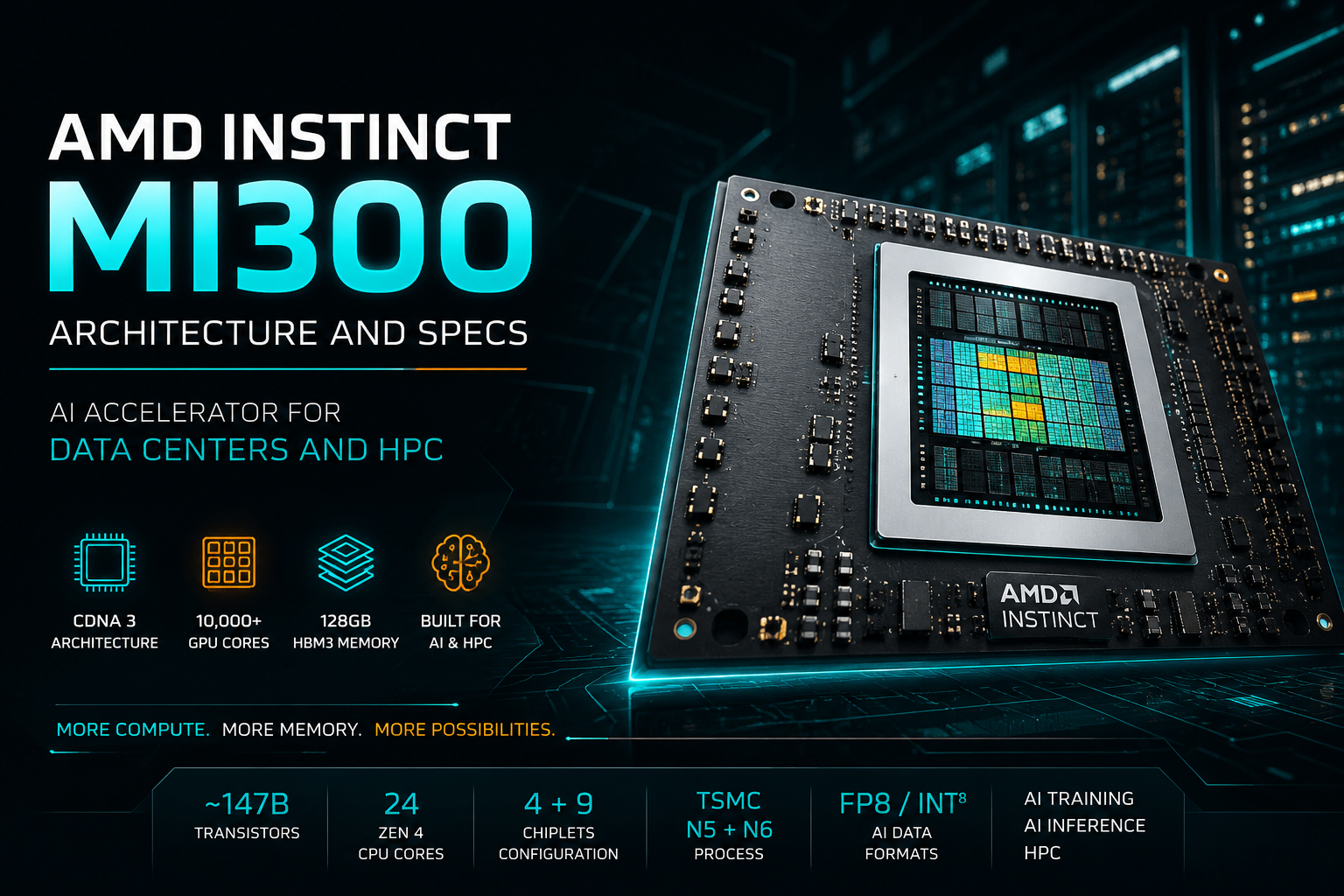
The MI300 is not a routine product update and it is not simply a larger GPU. It represents a major shift in how high-performance processors are designed for artificial intelligence and supercomputing. AMD built this platform around a new architectural approach that combines chiplets, advanced packaging, high-bandwidth memory, CPU and GPU integration, and AI-focused math performance in one package.
For readers following AI infrastructure, data center hardware, and the broader computing market, the MI300 matters because it shows what future accelerators will likely look like. It is a chip designed for an era where training and running AI models requires massive memory capacity, dense compute, and efficient interconnects at scale.
Why AMD Instinct MI300 Matters for AI and HPC Workloads
AI workloads have changed the rules of processor design. Large language models, recommendation systems, scientific simulations, and high-performance computing jobs all demand more than raw compute alone. They also require fast memory access, low-latency communication, and efficient scaling across many accelerators.
Traditional monolithic chip design struggles in this environment. Building one giant piece of silicon becomes increasingly difficult, expensive, and risky as complexity rises. Yields fall, manufacturing costs climb, and scaling becomes harder.
AMD’s answer was to move away from that old model and adopt a modular design philosophy. Instead of relying on one giant die, the MI300 uses multiple smaller dies that work together as a unified system. This chiplet-based strategy improves manufacturability, makes better use of advanced process nodes, and allows AMD to build more flexible high-performance products.
For AI infrastructure, that matters because modern accelerators are no longer judged only by peak compute. They are judged by how effectively they combine compute, memory, packaging, and system-level connectivity.
AMD Instinct MI300 Specifications and Core Hardware Features
| Specification | AMD Instinct MI300 |
|---|---|
| Architecture | CDNA 3 |
| Total Transistors | ~147 Billion |
| GPU Compute Cores | 10,000+ CDNA3 cores |
| CPU Cores | 24 Zen 4 cores |
| Memory Type | HBM3 |
| Memory Capacity | 128 GB |
| Chiplet Configuration | 4 base dies + 9 compute chiplets |
| Manufacturing Process | TSMC N5 + N6 |
| AI Data Formats | FP8, INT8 |
| Target Workloads | AI Training, AI Inference, HPC |
At a high level, the MI300 is an extremely large and ambitious processor package built for AI and HPC environments. The most important specifications mentioned in the source material are what make it so notable.
AMD Instinct MI300 key specs at a glance:
- 147 billion transistors
- More than 10,000 CDNA 3 GPU cores
- 24 Zen 4 CPU cores
- 128GB of HBM3 memory
- TSMC N5 and N6 process technologies
- A multi-chiplet design with four 6nm base dies and nine 5nm chiplets
- Advanced 2.5D and 3D packaging
- Support for low-precision AI math formats such as FP8 and INT8
These numbers immediately place the MI300 among the most complex processors ever built. Compared with earlier large accelerators from Intel and Nvidia, AMD’s design pushes transistor count and integration much further. But the important point is not just size. It is how AMD uses that silicon budget.
The MI300 combines GPU compute, CPU resources, large on-package memory, cache, and I/O into one tightly integrated structure. That combination is especially important for AI systems, where data movement can become just as limiting as arithmetic throughput.
CDNA 3 Architecture and AMD’s Move to Chiplet-Based GPU Design
The architectural foundation of the MI300 is CDNA 3, AMD’s data center GPU architecture aimed at AI and HPC workloads. This is the blueprint that defines how the chip handles massively parallel processing, memory access, and AI acceleration.
One of the most important ideas behind CDNA 3 is that AMD is no longer treating the GPU as a single large chip. Instead, it breaks the design into scalable building blocks that can be connected together inside one package.
That modularity is central to the MI300 story. It is what allows AMD to increase compute density while keeping the design practical from a manufacturing standpoint.
What is the XCD in AMD Instinct MI300?
The core building block inside the MI300 family is the XCD, or Accelerator Complex Die. This is essentially the main compute tile used to scale GPU performance.
Each XCD contains:
- 40 compute units
- Scheduling and control logic
- High-speed local cache
The easiest way to understand the XCD is to think of it as a standardized compute block that AMD can replicate across the package. In the MI300X configuration, AMD uses eight of these compute dies together with fast memory to create a very large GPU.
That leads to one of the most important specification points in the source article: the MI300X reaches 304 compute units, which is about 40 percent more than the previous MI250X. That is a major increase in compute density, and it shows how effective chiplet scaling can be in high-performance GPU design.
Advanced Packaging, 3D Stacking, and HBM3 Memory in MI300
One reason the MI300 is so significant is that the packaging technology is not just supporting the design. It is enabling it.
AMD combines 2.5D and 3D integration in the MI300 package. The HBM3 memory sits around the compute structure using interposer-based integration, while active compute and base dies are stacked in a true 3D arrangement.
This matters because modern accelerators are increasingly constrained by how quickly they can move data and power between functional blocks. Packaging is no longer a secondary engineering detail. It is now one of the core performance technologies in advanced chips.
MI300 chiplet layout and memory configuration
According to the provided source, the package includes:
- Four 6nm base chiplets
- Six 5nm CDNA 3 GPU compute chiplets
- Three 5nm Zen 4 CPU chiplets
- Eight 16GB HBM3 stacks for a total of 128GB
This arrangement allows AMD to separate functions intelligently. The base dies likely handle cache and I/O duties, while the upper compute chiplets focus on GPU and CPU processing. The result is a layered structure that delivers high compute density without depending on one impossibly large die.
From an AI hardware perspective, this is one of the most important trends in the industry. Future accelerators will increasingly depend on advanced packaging, not just smaller process nodes, to keep scaling.
AMD MI300 AI Performance for Training and Inference Workloads
| Accelerator | FP8 AI Performance | FP16 AI Performance | Memory Bandwidth |
|---|---|---|---|
| AMD MI300 | ~2600 TFLOPS | ~1300 TFLOPS | ~5.3 TB/s |
| Nvidia H100 | ~2000 TFLOPS | ~1000 TFLOPS | ~3.35 TB/s |
| AMD MI250X | N/A | ~383 TFLOPS | ~3.2 TB/s |
The most practical question is simple: what do these specifications actually mean for AI?
The answer starts with the data types used in machine learning. Many modern AI models do not need every operation to run at full high-precision scientific formats. Lower-precision formats such as FP8 and INT8 allow accelerators to process more operations per second while reducing bandwidth and power requirements.
AI Accelerator Comparison: AMD MI300 vs Nvidia H100 vs MI250X
| Feature | AMD MI300 | Nvidia H100 | AMD MI250X |
|---|---|---|---|
| Architecture | CDNA 3 | Hopper | CDNA 2 |
| Transistors | ~147 Billion | ~80 Billion | ~58 Billion |
| Memory Type | HBM3 | HBM3 | HBM2e |
| Memory Capacity | 128 GB | 80 GB | 128 GB |
| AI Precision Support | FP8, INT8 | FP8, FP16, INT8 | FP16, INT8 |
| Primary Use | AI + HPC | AI Training / Inference | HPC / Supercomputing |
| Target Systems | AI Data Centers | AI Clusters | Supercomputers |
That is why the MI300’s AI-focused numbers are so important.
MI300 AI performance highlights for FP8 and INT8
-
Up to 16x gain using newer low-precision methods compared with older approaches
-
More than 2,600 TFLOPS in FP8 and INT8-class workloads
-
Roughly 3x higher performance for important AI training formats
-
Nearly 7x gain for INT8 inference-focused performance
-
Up to 8x AI training performance and 5x AI power efficiency, according to AMD claims referenced in the source
These figures show that the MI300 is not merely a scientific computing processor that also happens to run AI. It is clearly tuned for machine learning acceleration.
For AI training, that means faster throughput on the matrix-heavy operations used in deep learning. For inference, it means improved efficiency when serving trained models in production. In practical data center terms, that can translate into fewer accelerators per deployment, lower energy cost per query, or faster time to train large models.
Unified Memory and APU-Style Integration
Another major feature highlighted in the source is the MI300’s move toward a more integrated APU or SoC-like structure. Instead of keeping CPU and GPU resources as separate devices that must communicate across longer board-level interconnects, AMD brings them together inside one package.
This provides two major benefits.
First, it reduces the amount of power wasted moving data between separate chips. In large AI and HPC systems, data movement can consume a surprising amount of energy. Shortening that distance improves both efficiency and latency.
Second, it supports a more unified memory model. When CPU and GPU elements share access to the same memory pool, software becomes easier to manage and data copies can be reduced. That can simplify programming while also improving system efficiency.
For AI infrastructure, this is a meaningful direction. As model sizes grow, reducing unnecessary memory duplication and data transfer becomes increasingly important.
How MI300 Fits Into Large AI Systems
One powerful accelerator is useful, but AI data centers depend on many accelerators working together as one system. That is where AMD’s Infinity Fabric becomes essential.
In the source material, eight MI300X accelerators are connected in a fully meshed topology inside a server node. This allows each GPU to communicate directly with the others using high-bandwidth, low-latency links.
That kind of connectivity is critical for distributed AI training. Large models often need to be split across multiple accelerators, and poor interconnect design can erase much of the benefit of faster chips. By allowing the GPUs to behave more like parts of one larger shared compute platform, AMD improves the usefulness of the raw compute and memory resources inside the node.
This is why accelerator design can no longer be separated from infrastructure design. In AI, the chip, the memory, the package, and the interconnect all matter at the same time.
The Software Hurdle: Can ROCm Truly Challenge the CUDA Empire?
The MI300 is undeniably a beast on paper, but in the real world, hardware is only half the battle. The real bridge for developers is the software ecosystem, and that’s where AMD’s open-source ROCm platform comes into play.
Right now, AMD is working overtime to make sure big names like PyTorch and TensorFlow run smoothly, so developers don't have to rewrite their entire codebase just to switch chips. Plus, the "Unified Memory" setup is a huge win—it cuts out the messy, complex data shuffling between the CPU and GPU, making life a lot easier for programmers.
But let's be honest: NVIDIA’s CUDA has a massive head start. It’s polished, deeply integrated, and has been the industry standard for years. Closing that gap is AMD's biggest challenge if they want to truly dominate the AI data center. While these software tools are what will ultimately make or break the platform, we’re keeping our focus in this article strictly on the "nuts and bolts"—the hardware architecture and those record-breaking specs.
Conclusion: What AMD Instinct MI300 Shows About the Future of AI Accelerators
The AMD Instinct MI300 is important because it combines several major trends in advanced computing into one platform. Its specifications are impressive on paper, but the deeper story is about integration. AMD is bringing together chiplets, 3D stacking, HBM3 memory, CPU and GPU resources, unified memory concepts, and AI-optimized math performance in a single package designed for large-scale computing.
From a hardware perspective, the MI300 shows that the future of AI accelerators will not be defined by one metric alone. Compute density matters, but so do memory capacity, packaging, data movement, and multi-GPU connectivity. That is the real lesson behind the MI300 architecture.
For AI data centers, supercomputers, and next-generation infrastructure, this kind of design is likely to become the norm rather than the exception. AMD is not just launching another accelerator. It is showing what the next phase of processor design looks like.
FAQ
Q1: What is AMD Instinct MI300?
AMD Instinct MI300 is a high-performance processor platform designed for artificial intelligence and high-performance computing. It combines GPU and CPU technologies, advanced packaging, and large HBM3 memory capacity in one package.
Q2: How much memory does the MI300 have?
The source article describes the MI300 as including 128GB of HBM3 memory, delivered through eight 16GB memory stacks.
Q3: Why is the MI300 important for AI?
It supports AI-friendly formats such as FP8 and INT8, offers very high throughput for training and inference, and is built to scale in large multi-GPU systems.
Q4: What makes MI300 different from older GPUs?
Its biggest differences are the chiplet design, 3D packaging, CPU and GPU integration, unified memory direction, and much stronger focus on AI acceleration.
Q5: What is the XCD in MI300?
XCD stands for Accelerator Complex Die. It is the core compute building block in the CDNA 3 architecture and contains compute units, cache, and control logic.
Q6: Is MI300 only for artificial intelligence?
No. It is also designed for scientific computing and other HPC workloads, but AI is clearly one of its main targets.
Q7: Why does packaging matter so much in MI300?
Because modern accelerators depend heavily on fast, efficient communication between compute dies and memory. Packaging is essential for delivering bandwidth, power efficiency, and scalability.
Q8: How does MI300 scale in data centers?
Multiple MI300X accelerators can be linked using Infinity Fabric in a high-speed mesh, allowing them to work together efficiently for large-scale AI training and inference.
Note: The prices shown are estimated market ranges based on industry reports and distributor listings. Actual prices can vary between suppliers and system integrators, and they often depend on order volume and contract terms. In general, AMD MI300 accelerators are estimated to range around $10,000–$15,000 while Nvidia H100 accelerators are commonly reported in the $25,000–$40,000 range depending on configuration and quantity. Large data center customers purchasing GPUs in bulk may receive significantly lower per-unit pricing.